
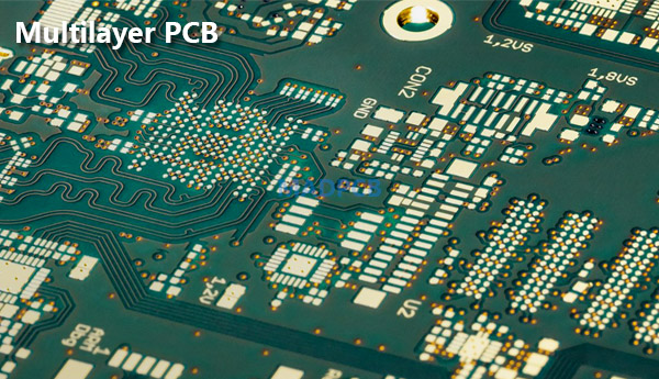
In the case of a large number of interconnection and crossover requirements, if the PCB circuit board wants to achieve a satisfactory performance, it must expand the board layer to more than 2 layers. Therefore, the original intention of the multi layer circuit board has appeared. It provides more freedom for the routing path.
The multi-layer circuit board has a layer of core material, and the copper layers are sequentially laminated on both sides using insulating prepreg. Multilayer PCB typically contain three or more copper conductive layers. The top and bottom layers look similar to a double-sided PCB, but have many circuit layers in the center. Internal layers with plated holes for interconnection (through, blind, buried). The copper layers are bonded together by a resin layer (prepreg, PP). Various IC electronic components are soldered on top or bottom layers of multilayer circuit boards by using different packaging techniques such as SMT and BGA.
The manufacturing process of multilayer circuit boards is more complicated and more expensive than single-sided and double-sided PCBs, and the cost of troubleshooting is high. But multilayer printed circuit boards support high-density wiring designs. There is no limit to the number of layers in a multi-layer PCB, which depends on the manufacturer’s production capacity. The thickness of the board will increase with the increase of the number of layers of the circuit board, so as to meet the diversified circuit design and packaging process for a wider range of applications. The number of layers of a multi-layer PCB is usually superimposed by an even number, and the manufacturing cost of the odd-numbered layers will increase significantly and problems such as rockers are prone to occur.
Our Advantages In Multilayer PCBs
JHDPCB has the world’s leading production equipments:We have introduced a variety of world-renowned production equipment, such as Orbotech LDI, VIGOR lamination machines, Mitsubishi laser drilling machines, Command plating lines, PTH Lines and etc.
Excellent procurement supply chain management: We reduce our material costs through centralized procurement and large-scale procurement.
Experienced team of experts: We have been deeply engaged in multilayer circuit board production for more than 12 years and grow into an industry-leading multilayer circuit board manufacturer, supported by an experienced team of experts that can provide our customers with reliable quality PCB.
Quick delivery: To shorten the delivery time. Everything is manufactured under one roof with our state-of-the-art equipment. We have many brands of laminate in stock, such as aluminum. Can deliver 3-5 days for sample order and 14-18 days for bulk order. More lead times can be found in “PCB Quick Turn”.
Rich experience in projects: Over the years, we have served various multi-layer projects in various industries, and manufactured the highest quality PCB projects for virtually every technology company, and we can do the same for you.
The Benefits of PCB Testing.
Find bugs: The main benefit of PCB testing is that it can effectively recognize bugs in the PCB. Whether the problem is functional, manufacturable, or otherwise, PCB testing identifies issues in PCB design and layout so designers can make adjustments accordingly.
Reduce costs: PCB testing prevents waste from producing defective products by using prototyping and small-quatities assemblies to test products. By accomplishing overall testing early in the design procedure, designers can prevent the bulk production of defective PCBs, in order to ensure the design is as perfect as possible before it goes into production This step helps to reduce production costs significantly.
Saves time: In the long run, early-stage PCB testing helps save time, to allow designers to recognize major problem during the prototyping step. Complete testing enables designers to quickly and easily discover the root cause of problems and make adjustments so they can continue production faster and reduce product lead times.
Reduced return rate: When a company conducts PCB testing, it can effectively reduce the chance of selling defective products or products that do not meet performance standards. This reduces costs associated with refunding customers and handling defective merchandise.In addition, reducing returns can make better customer satisfaction and company reputation enhanced.
Improved safety: Because PCBs are often used in fundamental electronics technology, their nonsuccess result in significant problems for a company’s productive forces or an Organizational skills. Defective PCBs may cause accidents such as fire, and in severe cases may cause injuries to nearby workers. Pre-manufacturing testing also ensures that machines and workers are not damaged or injured by improper design during production.
Although thorough testing of all types of PCBs is not required, especially ones that are already technically mature. But most new and custom PCB designs require regular testing of the design procedure. JHD provides customers with high quality and reliable PCBs by establishing proper PCB testing procedures for their needs.
More Stories
Schutts Industrial Heavy Duty Gas Struts for Every Application
How Enterprises Are Transforming Document Management with Integrated Portals
The Role of AI in Automating Compliance Monitoring for Remote Teams